ERS electronic Opens Demonstration Center in Zhubei to Meet Growing Demand for Panel-Level Packaging in Taiwan

ZHUBEI, Taiwan, May 8, 2025 /PRNewswire/ -- ERS electronic, the industry leader of thermal management solutions for semiconductor manufacturing, is excited to announce the opening of its latest demonstration center in Zhubei, Taiwan. This new facility will offer chipmakers and OSATs in Taiwan direct access to ERS's PhotoThermal debonding machine for wafers and panels, LUM600S1, a strategic move to meet the growing demand for panel-level packaging (PLP) technologies in the region.
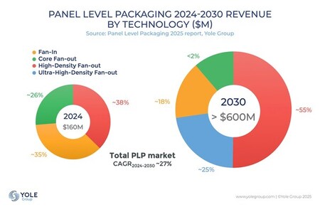 Source: Panel Level Packaging 2025 report, Yole Group
Panel-level packaging is rapidly gaining traction in the semiconductor industry due to its cost advantages and process scalability. Dr. Yik Yee Tan, Technology & Market Principal Analyst at Yole Group, predicts that the market will grow from $160 million in 2024 to over $600 million by 2030, driven by cost-efficient solutions in advanced packaging. By 2030, high-density fan-out technology, propelled by Generative AI, is expected to dominate the market, capturing more than 50% of the market share(1). In Chiplet and Heterogeneous Integration demand for larger form factor is driving the growth of PLP in the coming years to meet higher density requirement. For large package size of ~5.5x reticle size limit, PLP can boost carrier area efficiency by more than 80%, compared to just 45% with Wafer Level Packaging (WLP).
In addition to wafer solutions, ERS was among the first to bring PLP equipment to the market, introducing a panel-level debonder in 2018. Today, ERS offers a wide portfolio of semi- and fully-automatic systems, including PhotoThermal debonding machines enabling temporary bonding and debonding (TBDB) processes essential for handling ultra-thin substrates, which is critical for HPC and AI applications, like CoWoS and HBM.
"With LUM600S1, we are providing a high-yield solution tailored for high-volume manufacturing of complex AI chips. Our Taiwanese customers can now experience firsthand how PhotoThermal Debonding enhances efficiency, scalability, and cost-effectiveness," says Sébastien Perino, Managing Director of ERS Taiwan.
For more information about the Zhubei demonstration center and LUM600S1's availability for testing and demonstration, please visit ERS's website to get in contact with regional sales representatives.
About ERS:
ERS electronic GmbH, based in the Munich suburb of Germering, has been providing innovative thermal management solutions to the semiconductor industry for more than 50 years. The company has gained an outstanding reputation, notably with its fast and accurate air cooling-based thermal chuck systems for wafer probing. In 2008, ERS extended its expertise to the Advanced Packaging market. Today, their fully automatic and manual debonding and warpage adjust systems can be found on the production floors of most semiconductor manufacturers and OSATs worldwide.
(1) Sources: Panel Level Packaging 2025 report – Advanced Packaging Market Monitor, Yole Group
Photo - https://mma.prnasia.com/media2/2681597/PANEL_LEVEL_PACKAGING.jpg?p=medium600
Logo - https://mma.prnasia.com/media2/2614530/5306347/ERS_logo.jpg?p=medium600
PR Newswire Asia Ltd.

PR Newswire
1954年に設立された世界初の米国広報通信社です。配信ネットワークで全世界をカバーしています。Cision Ltd.の子会社として、Cisionクラウドベースコミュニケーション製品、世界最大のマルチチャネル、多文化コンテンツ普及ネットワークと包括的なワークフローツールおよびプラットフォームを組み合わせることで、様々な組織のストーリーを支えています。www.prnasia.com
本プレスリリースは発表元が入力した原稿をそのまま掲載しております。また、プレスリリースへのお問い合わせは発表元に直接お願いいたします。
プレスリリース添付画像


このプレスリリースには、報道機関向けの情報があります。
プレス会員登録を行うと、広報担当者の連絡先や、イベント・記者会見の情報など、報道機関だけに公開する情報が閲覧できるようになります。


