CKplas at SEMICON Japan : Enabling Your Advanced Packaging Now!
TOKYO, Dec. 5, 2024 /PRNewswire/ -- As Moore's Law almost reaches to its limits, advanced packaging will drive to the next leap in transistor density. The growing demand for AI chips is propelling this evolution of fan-out packaging technologies from wafer-level (FO-WLP) to panel-level (FO-PLP) for more chip integration in devices.
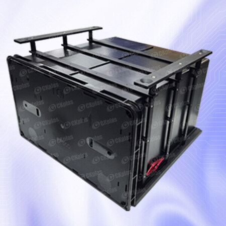 CKplas Panel FOUP 500mm
CKplas has been developing PCB/ABF FOUPs for over 20 years, leveraging decades of experience to seamlessly transition into the Panel FOUP market. Our supported substrates have expanded from wafers to glass. Over half of the world's top 10 PLP manufacturers are CKplas customers. In addition to Taiwan, our products are now in mass production and supplied to Japan, Korea, the United States, and Europe.
Seizing this market opportunity, CKplas will showcase its latest innovations in SEMICON Japan, held from December 11 to 13 at Tokyo Big Sight, East Hall 1, Booth #1828. We invite customers and industry partners to visit our booth for in depth discussions and to exchange valuable insights on the future of semiconductor technologies.
Media Contact
Lily Lin
TEL:+886-3-3185300
Mail:mkt@ckplas.com
PR Newswire Asia Ltd.

PR Newswire
1954年に設立された世界初の米国広報通信社です。配信ネットワークで全世界をカバーしています。Cision Ltd.の子会社として、Cisionクラウドベースコミュニケーション製品、世界最大のマルチチャネル、多文化コンテンツ普及ネットワークと包括的なワークフローツールおよびプラットフォームを組み合わせることで、様々な組織のストーリーを支えています。www.prnasia.com
本プレスリリースは発表元が入力した原稿をそのまま掲載しております。また、プレスリリースへのお問い合わせは発表元に直接お願いいたします。
プレスリリース添付画像


このプレスリリースには、報道機関向けの情報があります。
プレス会員登録を行うと、広報担当者の連絡先や、イベント・記者会見の情報など、報道機関だけに公開する情報が閲覧できるようになります。


